


Microlens Arrays: Versatile and Efficient
Microlens Arrays: Design, Fabrication and Applications
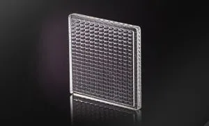
Microlens arrays are compact optical components consisting of numerous miniature lenses arranged in one- or two-dimensional patterns. By precisely controlling and redistributing light, microlens arrays improve optical efficiency and enable advanced functionalities in imaging, beam shaping, optical sensing, and illumination systems.
These arrays can be manufactured in circular, square, or hexagonal geometries and are commonly fabricated on fused silica or optical glass substrates. Their compact size, high fill factor, and excellent optical performance make them important components in modern optical engineering.
Design and Composition of Microlens Arrays
Microlens arrays may be produced as individual optical components or integrated into larger optical systems. Depending on the application, they can be mounted in metal or polymer structures for easier alignment and integration.
Each array may contain thousands or even millions of microlenses arranged in grids, rectangles, or circular patterns. Important design parameters include:
- Lens pitch
- Focal length
- Fill factor
- Lens geometry
- Surface quality
- Transmitted wavefront quality
Most microlens arrays are manufactured from UV fused silica, which offers excellent transmission across ultraviolet, visible, and infrared wavelengths. Their high fill factor helps reduce zero-order hot spots and improve uniformity in illumination systems.
Optical Characteristics of Microlens Arrays
Microlens arrays provide several important optical advantages, including:
- Large field of view
- High optical efficiency
- Low aberration and distortion
- Uniform light distribution
- High fill factor
- Excellent beam homogenization capability
These characteristics make microlens arrays particularly suitable for applications requiring precise light management and high optical efficiency.
Advanced Fabrication Techniques
The fabrication of microlens arrays differs significantly from traditional lens manufacturing due to their small dimensions and dense arrangement.
Most microlens arrays are fabricated using semiconductor processing technologies, allowing all lenses within the array to be manufactured simultaneously with high precision.
Common Fabrication Methods:
- Photolithography: Photolithography uses a predefined lens pattern created by a photomask to define the geometry of each microlens with high accuracy.
- Etching Techniques: Chemical or plasma etching techniques are used to shape the microlenses directly into the substrate.
- Hot Embossing and Printing: These methods rely on the surface tension of heated materials to form the desired lens profiles and are commonly used for high-volume production.
- Laser Materials Processing: Laser-based fabrication creates microlenses individually with excellent flexibility and precision, although it is generally more expensive than batch manufacturing methods.
Applications of Microlens Arrays
Microlens arrays are widely used in:
- 3D Imaging and Light Field Cameras
- Beam Shaping and Beam Homogenization
- Fiber Coupling and Optical Communication
- LiDAR and Optical Sensors
- Medical Devices
- Wavefront Sensors
- Laser Optics
- Metrology Systems
1. Imaging Systems
Microlens arrays improve light collection efficiency and image quality in:
- CCD arrays
- CMOS sensors
- Light field cameras
- 3D imaging systems
- Optical microscopes
2. Beam Homogenization and Beam Shaping
Microlens arrays are widely used to homogenize and shape laser beams, creating highly uniform illumination profiles.
Applications include:
- Laser welding
- Laser drilling
- Laser ablation
- Fluorescence microscopy
- Semiconductor instrumentation
Fly’s eye condenser arrays, composed of dual-surface cylindrical microlenses, are commonly used for flat-top beam generation and uniform illumination.
3. LiDAR and Optical Sensing
Microlens arrays are important components in LiDAR and optical sensing systems, where they help improve:
- Beam shaping
- Optical efficiency
- Signal collection
- Light distribution
- Sensor performance
These properties make them valuable in autonomous vehicles, machine vision, and optical sensing technologies.
4. Shack-Hartmann Wavefront Sensors
Microlens arrays are used in Shack-Hartmann wavefront sensors to measure the wavefront shape of incident light.
These sensors are widely employed in:
- Adaptive optics
- Astronomical telescopes
- Laser diagnostics
- Optical testing systems
5. Light Field Cameras
In light field cameras, microlens arrays are positioned between the primary lens and the image sensor.
This arrangement enables:
- Post-capture refocusing
- Depth extraction
- Multi-perspective imaging
- Computational photography
Conclusion
Microlens arrays have become essential optical components for controlling, redistributing, and shaping light in modern optical systems. Their unique ability to improve optical efficiency and enable advanced imaging and sensing capabilities has made them indispensable across applications ranging from microscopy and LiDAR to beam shaping and computational imaging.
As fabrication technologies continue to advance, microlens arrays are expected to play an increasingly important role in the development of next-generation optical systems.
Need a Custom Microlens Array for Your Optical System?
Whether you are developing an imaging system, LiDAR platform, beam homogenizer, or optical sensing application, Shanghai Optics can provide custom microlens arrays tailored to your technical requirements.
Contact us to discuss your project or explore our Microlens Array product specifications.


