


Custom High-NA Objectives for Advanced Logic Node Wafer Inspection & Metrology
- Cylindrical Lenses
- Aspheric Lenses
- Achromatic Lenses
- Spherical Lenses
- Optical Prisms
- Optical Mirrors
- Beamsplitters
- Optical Windows
- Infrared Optics
- Micro Optics
- Optical Filters
- Colored Glass Filters
- Custom Shapes
- Laser Optics
- Freeform Optics
- Fresnel Lenses
- Light Pipe Homogenizing Rods
- TIR Lens
- Medical Device Optics
Custom High-NA Objectives for Advanced Logic Node Wafer Inspection & Metrology
As semiconductor manufacturing advances to increasingly complex logic nodes, inspection and metrology systems face tighter requirements for defect sensitivity, measurement repeatability, and throughput. The challenge is not simply achieving higher numerical aperture (NA), but maintaining the required field of view (FOV), working distance (WD), wavefront performance and system stability at the same time.
For optical engineers developing next-generation inspection and metrology instruments, these parameters must be balanced within an objective that can actually be fabricated, aligned, tested and reproduced.
Shanghai Optics works with R&D teams and instrument OEMs to design and manufacture custom high-NA objective lenses and precision optical assemblies for advanced wafer inspection and metrology systems—from optical design and tolerance analysis through fabrication, coating, alignment, assembly and verification.
The Real Advanced Logic Node Challenge: High NA Without Sacrificing FOV, WD and Stability
At advanced process nodes, pushing NA alone does not produce an effective inspection objective.
Increasing NA places tighter constraints on element decenter, tilt, air spacing, surface figure and focus stability. At the instrument level, these requirements must also be balanced against usable FOV, wafer clearance, illumination geometry, detector format and inspection throughput.
For a custom wafer inspection objective, the design space can involve simultaneous control of:
- High NA and usable working distance
- Wide FOV and off-axis performance
- UV or multi-wavelength aberration correction
- Wavefront error and MTF
- Low distortion and telecentricity error
- Element decenter, tilt and axial spacing
- Stray light and surface scatter
- Thermal and mechanical stability
- Objective barrel and instrument interface
Shanghai Optics evaluates these parameters together during optical design and tolerance analysis to establish a manufacturable performance envelope before fabrication.
Target Specifications for Advanced Wafer Inspection
The most useful objective specification is not an isolated maximum NA, wavelength or working distance. For an inspection instrument, the critical question is which performance parameters can be achieved simultaneously within one manufacturable objective architecture.
| Parameter | Target / Achievable Specification |
| Numerical Aperture (NA) | 0.90–1.35 |
| Operating Wavelength / Spectral Range | 193 nm DUV / 248 nm / 355 nm UV / Visible / NIR |
| Working Distance (WD) | 0.5–5 mm for high-NA designs; >10 mm achievable for long-working-distance configurations |
| Field of View (FOV) | 0.5–3.5 mm |
| RMS Wavefront Error | < λ/14; target RMS WFE < 0.05λ |
| MTF | >0.4–0.5 contrast at the specified spatial frequency |
| Distortion | <0.1–0.5% across the full field |
| Telecentricity | <2 mrad object-side; <5 mrad for standard configurations |
| Surface Quality | 20-10 scratch-dig typical; 10-5 available for critical UV/DUV surfaces |
| Surface Roughness | ≤0.5 nm RMS for visible/NIR; ≤0.2–0.3 nm RMS for UV/DUV |
| Centration / Decenter | ≤2–5 µm decenter; ≤5–10 arcsec tilt, depending on element and design |
| Objective Configuration | Dry (NA ≤0.9) and immersion (NA >1.0) configurations; final architecture application-dependent |
| Optical Materials | UV-grade fused silica, CaF₂, and low-dispersion optical glasses selected according to spectral and thermal requirements |
| Coating | Broadband or multi-wavelength AR coatings; low-scatter and high-LIDT coatings available for UV/DUV applications |
| Operating Temperature / Thermal Stability | 20–25°C, typically ±0.5°C; ±0.1°C for high-stability metrology systems; athermalized designs available |
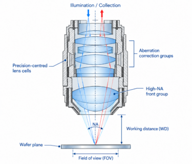
Balancing NA, FOV and Working Distance
NA, FOV and WD create one of the central trade spaces in high-performance objective development.
Increasing NA can improve collection efficiency and spatial-frequency response, but it also increases sensitivity to aberrations and assembly tolerances. Extending the working distance while maintaining high NA places additional constraints on front-group geometry and mechanical packaging. Increasing FOV simultaneously increases the burden on off-axis aberration and distortion control.
For instrument development, Shanghai Optics optimizes these parameters together rather than maximizing one specification independently.
| Design Requirement | Engineering Impact |
| Higher NA | Tighter aberration, centering, spacing and focus tolerances |
| Larger FOV | Greater demand on coma, astigmatism, field curvature and distortion correction |
| Longer WD | More constrained high-NA geometry and mechanical packaging |
| Shorter Wavelength | Tighter material, coating, surface figure and scatter requirements |
| Low Distortion | Increased importance of field-dependent optimization |
| Low Wavefront Error | Tighter fabrication, centering and assembly tolerance budgets |
The resulting objective architecture is therefore driven by the performance required at the instrument level—not by a single headline specification.
UV and Multi-Wavelength Aberration Control
Advanced wafer inspection may use UV, visible or NIR wavelengths depending on the defect type, material stack and measurement architecture.
For UV-sensitive objectives, material selection becomes increasingly restrictive as wavelength decreases. Synthetic fused silica, CaF₂ and other application-specific materials can be evaluated based on transmission, dispersion, thermal behaviour, coating compatibility and manufacturability.
Multi-wavelength systems introduce additional constraints on axial and lateral colour correction while maintaining wavefront performance across the required FOV. These requirements must be balanced against element count, transmission, mechanical envelope and tolerance sensitivity.
Rather than forcing an extremely broad spectral range into a single objective, Shanghai Optics can optimize the optical prescription, material combination and coating around the wavelengths actually required by the instrument.
Designing for Manufacturability
A high-performance optical model is only useful if its predicted performance survives fabrication and assembly.
High-NA objectives can be particularly sensitive to small variations in element position and geometry. Shanghai Optics incorporates tolerance analysis into the design process to identify the parameters that have the greatest impact on final system performance.
Depending on the architecture, tolerance analysis can evaluate:
- Element decenter and tilt
- Centre thickness
- Air spacing
- Surface figure
- Radius tolerance
- Wedge
- Refractive index variation
- Barrel and cell positioning
- Assembly alignment
- Thermal variation
This allows optical performance to be evaluated against realistic fabrication and assembly tolerances before the design is released for manufacturing.
Where necessary, compensators and alignment strategies can be incorporated into the assembly process to maintain the required system performance.
Optomechanical Stability Under High-Throughput Operation
In a production inspection instrument, objective performance must remain stable beyond the optical bench.
Repeated stage motion, vibration, instrument warm-up and thermal variation can introduce small changes in lens spacing, centering, tilt or objective position. At high NA, these changes can affect focus, wavefront performance and measurement repeatability.
The objective barrel therefore needs to be treated as part of the optical tolerance budget rather than simply as a mechanical enclosure.
Depending on the system requirements, Shanghai Optics can integrate:
- Low-CTE structural materials
- Precision-centred lens cells
- Controlled axial spacing
- Stress-minimized lens mounting
- Thermal-mechanical analysis
- Stable objective-to-instrument interfaces
- Application-specific alignment strategies
Optical and mechanical tolerances can then be evaluated together before the objective progresses into prototype manufacturing.
From Optical Prescription to Verified Assembly
For R&D teams and instrument OEMs, one of the largest development risks occurs between the optical model and the assembled objective.
Performance can be lost through surface fabrication error, coating variation, centering error, element spacing or mechanical assembly—even when the nominal optical design performs well.
Shanghai Optics supports the complete objective development path through:
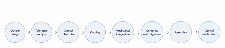
Depending on the project, final acceptance criteria can include:
- MTF
- RMS wavefront error
- Distortion
- Telecentricity
- Field performance
- Spectral transmission
- Surface figure
- Surface quality
- Centration
- Focus stability
Defining these acceptance criteria during the design stage helps maintain continuity between simulation, manufacturing and final system performance.
Built for R&D and Instrument Integration
Shanghai Optics develops custom objectives for optical engineers and R&D teams whose system requirements cannot be met with an off-the-shelf objective. Our experience with custom objectives for semiconductor manufacturing supports applications ranging from wafer inspection and metrology to other advanced semiconductor optical systems.
For advanced wafer inspection and metrology, this can include architectures such as:
- Brightfield and darkfield inspection
- Optical metrology
- Multi-wavelength inspection
- Advanced packaging inspection
- 3D IC and chiplet inspection
- TSV inspection
- Precision optical characterization
For model-based metrology architectures, the objective can be optimized around illumination delivery, collection efficiency, polarization behaviour, wavefront quality and measurement repeatability rather than direct imaging resolution alone.
This distinction is important for angstrom-era applications: the process-node designation does not mean that an optical objective directly resolves a 3 nm feature. Instead, the objective must provide the stable and well-characterized optical performance required by the complete inspection or metrology instrument.
From R&D Prototype to Production
A custom objective developed for an R&D platform may ultimately need to transition from several prototypes into a repeatable production assembly.
Shanghai Optics supports this development path from optical and optomechanical design through prototype fabrication, alignment, testing and production manufacturing.
Customers can provide an existing optical prescription for manufacturing review or work with our engineering team from system-level requirements.
For a new custom objective, useful starting inputs include:
- Operating wavelength or spectral bands
- Target NA
- Required working distance
- Field of view
- Detector format and pixel size
- MTF or wavefront requirements
- Distortion and telecentricity limits
- Illumination and collection geometry
- Mechanical envelope
- Mounting interface
- Thermal and environmental requirements
- Prototype and production quantities
Engineer Your Next High-NA Objective with Shanghai Optics
For advanced wafer inspection and angstrom-era metrology instruments, high NA is only one part of the design challenge. FOV, working distance, spectral performance, wavefront quality, manufacturing tolerances and optomechanical stability must perform together within a repeatable assembly.
Shanghai Optics works with R&D teams and instrument OEMs from optical design and feasibility analysis through precision manufacturing, coating, alignment, assembly and testing.


