
Seeing the Invisible: Overcoming Design Challenges in Near-Infrared (NIR) Optical Systems
In precision optics, the boundaries of visible light often double as physical limitations. For engineers and researchers across industrial manufacturing, semiconductor fabrication, and life sciences, critical structural data is frequently trapped beneath the surface—hidden behind silicon wafers, opaque substrates, or thick biological tissue.
Custom Near-Infrared (NIR) microscopy systems, optimized for the 780nm to 2500nm wavelength range, bypass these limitations. By leveraging specialized coatings and advanced optical substrates, custom microscope objectives allow teams to non-destructively peer through previously impenetrable barriers.
However, translating raw infrared performance into a high-throughput industrial system requires balancing aggressive optical specifications with severe manufacturing realities.
Subsurface Imaging: Piercing Opaque Barriers Non-Destructively
The primary advantage of NIR wavelengths lies in their unique interaction with matter. Materials that completely scatter or absorb visible light often become highly transparent when exposed to short-wave infrared (SWIR) and NIR radiation.
For advanced inspection teams, this capability shifts quality control from a destructive sectioning process to an efficient, non-destructive imaging workflow. Instead of physically cutting a sample to inspect an internal layer—which destroys the component and introduces structural artifacts—NIR light penetrates the material seamlessly. It uncovers subsurface anomalies, internal stratification, and structural voids while leaving the target entirely intact.
Cross-Industry Applications: Tailoring Optics to Specific Intent
To deliver crisp performance, an objective lens system must be tailored precisely to its environmental and industrial application.
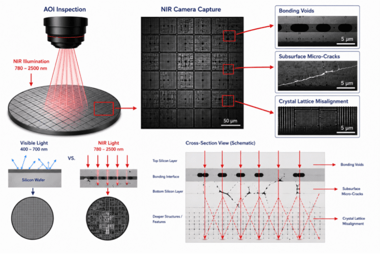
Semiconductor Inspection & Advanced Manufacturing
In modern chip fabrication and Micro-LED manufacturing, surface-level inspection is no longer sufficient. Visible light automated optical inspection (AOI) systems easily catch surface scratches, but they cannot evaluate internal bonding integrity.
Because silicon becomes optically transparent at wavelengths greater than 1050nm, custom-designed, infinity corrected objectives can image directly through the substrate. This allows quality control engineers to identify critical hidden defects, including:
- Subsurface micro-cracks and stress fractures
- Bonding voids in multi-layer wafer stacks
- Crystal lattice misalignments
Optimized with a high numerical aperture (NA≥0.35)and flat-field achromatic correction, these systems achieve crisp subsurface resolution down to 1.2 μm. This ensures high-throughput defect detection without sacrificing accuracy.
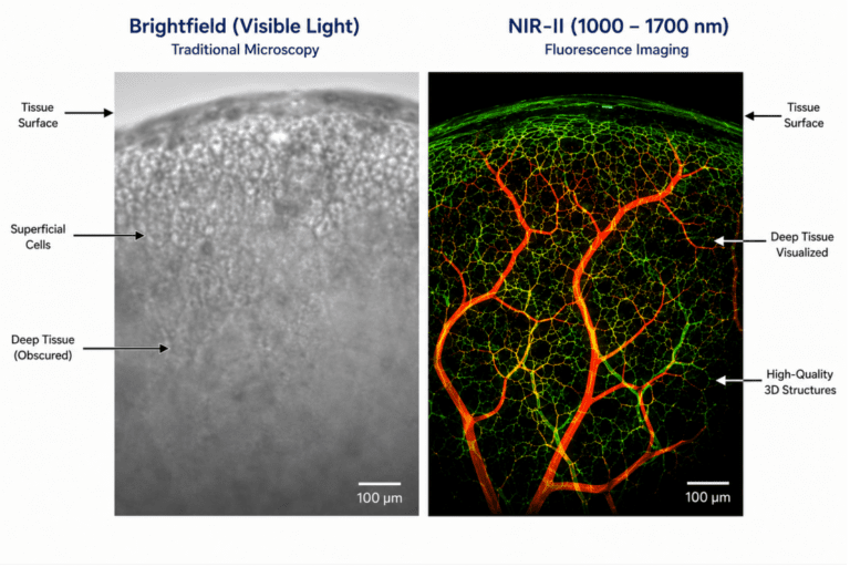
Biomedical Research & Deep-Tissue Bio-Imaging
In life science applications, imaging depth has traditionally been limited by light scattering and cellular phototoxicity. Traditional visible-light microscopy scatters rapidly, limiting clear imaging to the outermost cellular layers.
The NIR-II imaging window (1000nm to 1700nm) solves this dilemma. Biological tissues exhibit significantly lower light attenuation and minimal autofluorescence in this band. Utilizing specialized multi-immersion or water immersion objective lenses with broadband anti-reflective (AR) coatings, life science researchers can perform high-resolution 3D reconstructions of deep-seated vascular networks and tumor morphologies deep within intact tissues, maximizing signal-to-noise ratios.
Engineering Frontiers: Overcoming Severe Manufacturing Challenges
While the benefits of NIR imaging are clear, developing high-transmittance, aberration-corrected hardware presents severe design and production hurdles. Standard optical glass lacks the necessary transmittance in the upper NIR and SWIR bands, forcing optical engineers to innovate across materials science and optomechanical design.
| Engineering Obstacle | Industrial Solution for Custom Objectives |
| Substrate Absorption & Signal Loss | Standard optical glass absorbs NIR wavelengths. We utilize advanced crystalline materials, such as Chemical Vapor Deposition (CVD) Zinc Sulfide (ZnS), to maintain index uniformity (±0.00015). |
| Secondary Spectrum & Spherical Distortions | Broadband imaging from visible to NIR creates severe aberrations. We engineer complex, multi-element lens groupings (e.g., anti-telephoto structures) to flatten the field of view. |
| Maintaining Working Distances | High-magnification systems naturally compress spacing. We focus on specialized long working distance objectives (≥6mm) to protect delicate silicon wafers and biological samples. |
| Thin-Film Coating Stress | Multi-layer AR coatings face high internal stress, risking delamination. We deploy specialized plasma-assisted deposition to guarantee ultra-high transmittance (≥88%) across target bands. |
Shanghai Optics: Your High-Precision Custom Microscope Objective Supplier
At Shanghai Optics, we bridge the gap between complex optical physics and practical industrial reliability. We understand that manufacturing clients need build-to-print scalability, reliable pricing, and strict adherence to geometric tolerances, while R&D teams require rigorous performance verification.
Backed by over 20 years of precision manufacturing experience, we specialize in:
- Custom Microscope Objectives: Built to your exact mechanical envelope and spectral requirements.
- High-Aperture & High-NA Systems: Optimized for maximum light-gathering efficiency.
- Precision Lens Assemblies: Fully aligned and tested utilizing laser interferometry to ensure an RMS wavefront error <λ /5.
Whether you are optimizing an automated semiconductor inspection system or developing the next generation of deep-tissue bio-imaging platforms, our engineering team delivers the high-transmittance, aberration-corrected optics your project demands.
Request a quote or technical consultation for your custom objective project.